
MicroLED technology has been hailed as the next big leap in display innovation. With its ability to deliver higher brightness, better contrast, lower power consumption, and a longer lifespan compared to OLED and LCD, it is positioned to revolutionize industries from consumer electronics to automotive displays.
However, one critical bottleneck remains: MicroLED mass transfer — the process of moving millions of microscopic LEDs from their fabrication wafers to a target substrate with extreme precision and high yield. This step is arguably the most complex challenge preventing large-scale commercialization.
Mass transfer involves placing each micro-LED chip (often smaller than 100 micrometers) onto a backplane with precise alignment. This must be done for millions of pixels in a display while ensuring electrical connectivity and functional integrity.
Key requirements of MicroLED mass transfer include:
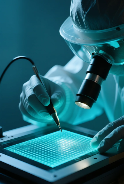
Unlike conventional LED placement for signage, MicroLED displays require positioning accuracy at a micron or even sub-micron level. For a 4K TV, that means correctly placing over 24 million RGB micro-LED chips. Even a 0.1% misplacement rate results in thousands of dead pixels.
Industry example:
Apple’s rumored MicroLED watch project is reportedly facing delays due to the difficulty of scaling precision without sacrificing production speed.
Yield directly impacts cost. If even a small fraction of chips fail during transfer, the entire panel may need rework or replacement. Achieving yields above 99.999% is essential for cost-effective production.
Some companies are experimenting with self-healing pixel architectures or redundant LEDs per pixel to mitigate yield issues — but these solutions increase design complexity.
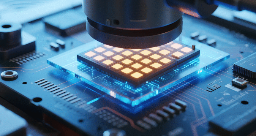
Current MicroLED mass transfer techniques require expensive machinery, custom equipment, and advanced robotics. Processes such as laser lift-off, fluidic self-assembly, and elastomer stamp transfer each have their own trade-offs in cost, speed, and precision.
Compared to OLED manufacturing, MicroLED fabrication still has a higher capex and opex due to:
One promising approach uses elastomeric stamps to pick up and place thousands of micro-LEDs simultaneously. Companies like PlayNitride and X-Celeprint are developing scalable versions of this technology, although issues with stamp wear and release accuracy remain.
Laser-induced forward transfer (LIFT) can move micro-LEDs with high precision by releasing them from the growth substrate using controlled laser pulses. This method reduces mechanical stress but requires careful thermal management to prevent chip damage.
This technique relies on surface tension and capillary forces to guide micro-LEDs into pre-patterned sockets on the target substrate. While potentially low-cost, it currently lacks the precision needed for high-resolution displays.
To counter low yields, some manufacturers integrate redundancy — multiple micro-LEDs per pixel — or develop pixel-level repair tools that can replace defective chips after transfer.
Even with challenges, the interest in MicroLED displays is strong due to their advantages:
Apple has been investing heavily in MicroLED research, reportedly aiming to replace OLED in its Watch lineup. Sources suggest that MicroLED mass transfer remains the biggest bottleneck, particularly in miniaturizing the process for small wearable screens while maintaining yield and controlling costs.

Q1: Why is MicroLED mass transfer so difficult?
Because it requires moving millions of tiny chips with micron-level precision at industrial speeds without damaging them.
Q2: Which industries will benefit most from MicroLED technology?
Consumer electronics, automotive, defense, and AR/VR will see the earliest adoption.
Q3: Is MicroLED cheaper than OLED?
Not yet. Manufacturing complexity and low yields make MicroLED currently more expensive, but costs are expected to drop with process improvements.
Q4: How long until MicroLED becomes mainstream?
Analysts estimate 3–5 years for wider adoption in premium products, with cost reductions coming as mass transfer technology matures.
MicroLED offers unmatched display quality, but without a breakthrough in mass transfer, it risks staying a niche technology. The race is on for manufacturers to balance precision, yield, and cost to unlock its full potential. With tech giants like Apple investing billions, it’s only a matter of time before these hurdles are overcome — and the display market may never look the same again.